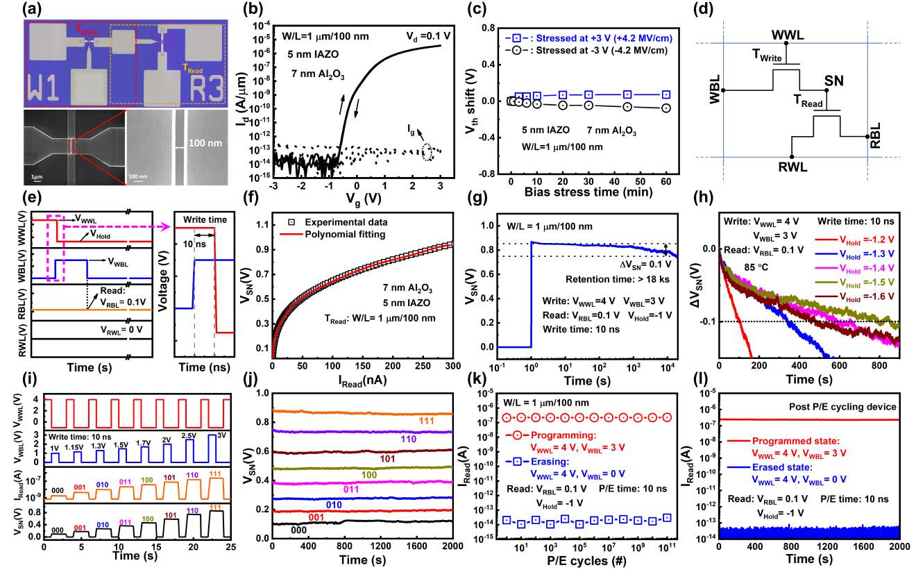
Our research group reported a high-performance 2T0C DRAM based on InAlZnO FETs.
With advancements in information technology, optimizing the performance of dynamic random-access memory (DRAM) has become crucial for technological progress. Traditional DRAM cells face limitations due to capacitor constraints, resulting in reduced data retention time and power performance. Therefore, exploring new DRAM architectures to fundamentally improve performance is significant. Oxide semiconductor field-effect transistors, with their wide bandgap, extremely low off-state current, and back-end-of-line (BEOL) compatibility, show great potential for single-chip 3D integration applications in 2T0C DRAM.
Using plasma-enhanced atomic layer deposition (PEALD) technology, our group fabricated thin-film transistors with InAlZnO (IAZO) nanoscale films as the channel and atomic layer-deposited Al2O3 films as the passivation layer. After annealing the device in nitrogen at 400°C for 60 minutes, there was almost no observable change in the transfer characteristics. Additionally, the device demonstrated excellent bias stress stability, with threshold voltage shifts of 0.07 V and -0.08 V after 60 minutes of +3 V and -3 V gate bias stress, respectively. Ultimately, our team showcased a 2T0C DRAM storage cell based on 100 nm short-channel IAZO FETs, achieving a write speed of 10 ns, over 18000 s of data retention time at room temperature, and over 1011 programming/erase cycles with no significant performance degradation. By controlling the write bit line voltage, we achieved 3-bit multilevel storage characteristics, with a uniform storage node voltage (VSN) distribution and sufficiently large spacing between adjacent states. This research provides a new development path for future DRAM storage technology. The related papers are published in IEEE Trans. Electron Devices (https://doi.org/10.1109/TED.2024.3365457) and Sci. China Inf. Sci. (https://engine.scichina.com/doi/10.1007/s11432-024-4112-x).
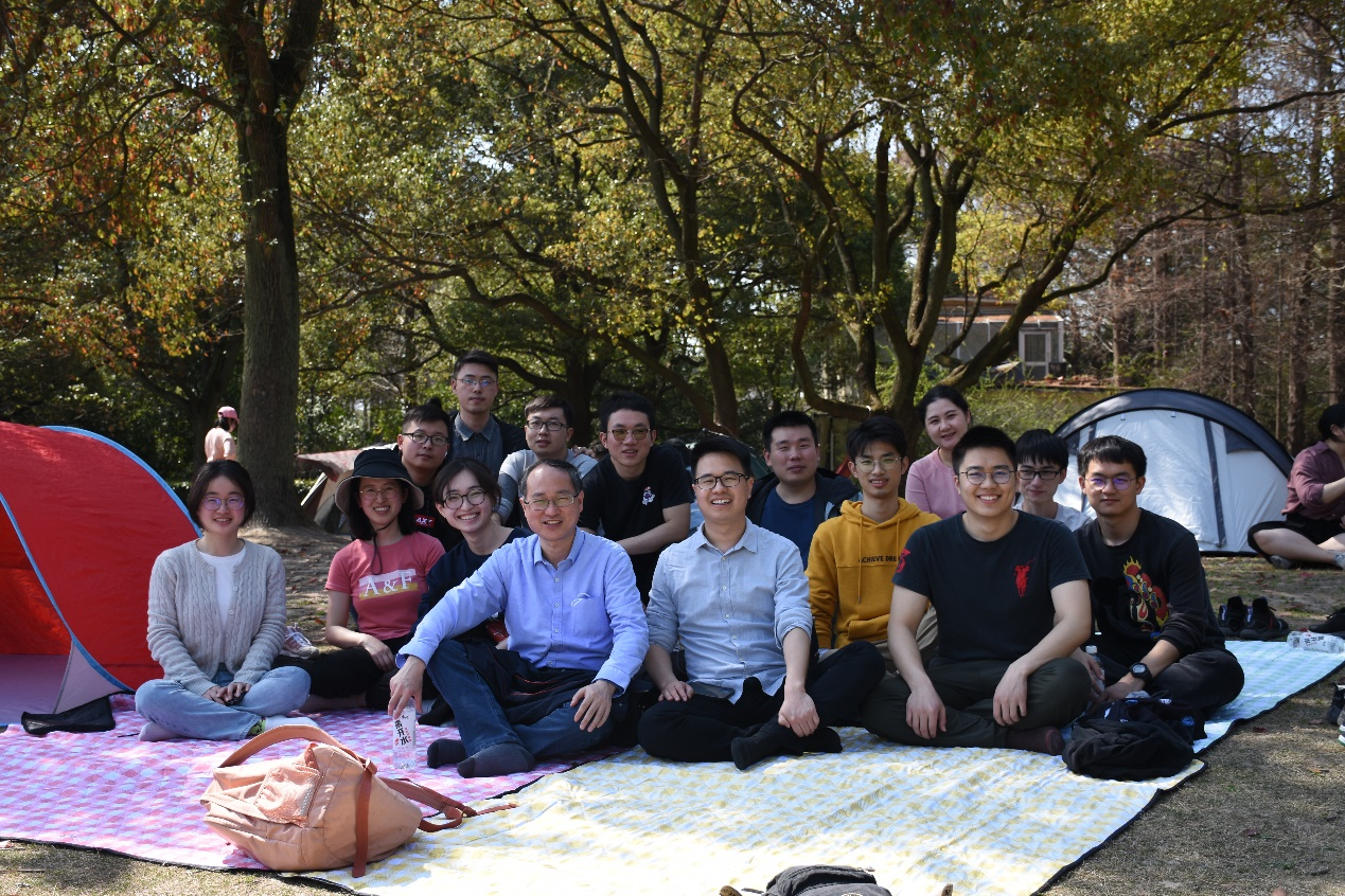
[Group activities] Shanghai Gongqing Forest Park-Sunshine Walk, Happy Tour
On March 12, 2022, the sun is shining and spring is in full bloom. It is a good time for outing. Our group organized a spring outing, which was enjoyed by all teachers and students.


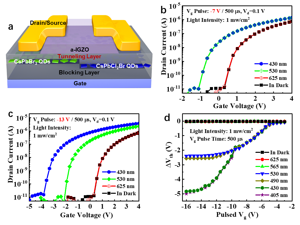
Ding Shijin's group reported an oxide semiconductor thin film transistor with optoelectronic logic and storage functions.
Optical signal has the advantages of high bandwidth, no Joule heat, high speed and low interference. The new computing architecture with the integration of photon and electron transmission is expected to become the key technology to overcome the bottleneck of Moore's Law in the field of integrated circuits. In recent years, with the development of optoelectronic mixed signal algorithm and silicon optical technology, the integration of photons and electronic computing units to the device level, thus further improving the performance of optoelectronic fusion chip system. Therefore, based on the concept of integration of storage and calculation, it is of great significance to develop a new type of multi-functional optoelectronic devices.
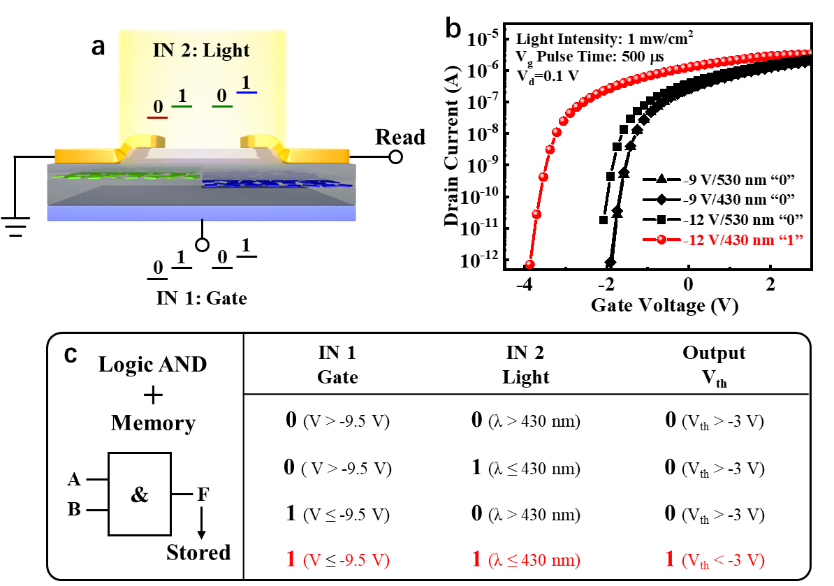
To meet the above requirements, Ding Shijin's research team adopts a ladder perovskite quantum dot floating gate and supports the device structure of amorphous IGZO thin film transistor to realize the function of polymorphic deposit fusion based on optoelectronic signal operation. The related work is published in ACS Nano magazine under the title of "Photoelectric Logic and In Situ Memory Transistors with Stepped Floating Gates of Perovskite Quantum Dots". The corresponding authors of this article are Ding Shijin and Wu Xiaohan, and the first author is Dr. Pei Junxiang.
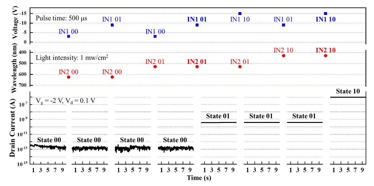
The device uses perovskite quantum dots with different band gaps as the charge trapping layer and photogenerated carrier layer in the stepped floating gate, so it can show the polymorphic non-volatile memory performance of programming or erasing both electric signal and high-bandwidth optical signal (Figure 1). By programming with bias and optical wavelength signals, the device can also achieve logic operations based on optoelectronic mixed signals (Figure 2). Combined with the above functions, the device can further demonstrate the fusion of multi-level logic operation and in-situ storage (Figure 3), so it has a wide application prospect in the next generation optoelectronic fusion chip system.
Original link: https://pubs.acs.org/doi/10.1021/acsnano.1c08945
In September 2021, our group reported that a flexible and high-performance flexible body gas sensor based on sub-molecular layer deposition technology
Organic semiconductor gas sensor has the advantages of controllable gas selectivity and intrinsic flexibility. It has a wide application prospect in intelligent sensing and Internet of things systems. However, its application is still faced with the problems of insufficient response speed and detection sensitivity. The gas sensor based on ultra-thin organic semiconductor film has ultra-high specific surface area, which can effectively improve the gas detection sensitivity and response speed of the device. However, it is difficult to prepare high quality ultra-thin organic semiconductor films by traditional processes, such as hot evaporation and solution spin coating. Atomic layer deposition process is based on the chemical mechanism of self-limiting reaction and has accurate controllability of atomic layer thickness, so it is widely used in integrated circuits, atomic catalysis, energy devices and other fields. The "molecular layer deposition process" for accurate and controllable preparation of polymer films by using this method has also been reported. However, the polymerization processes of most organic semiconductors, including polythiophene, polypyrrole and polyaniline, are based on functional group coupling reactions and do not have the characteristics of self-limiting reactions. Therefore, the development of molecular layer deposition process for organic semiconductors is still facing challenges.
In order to solve the above problems, our group developed the molecular layer deposition process of polythiophene thin film for the first time, and developed a high performance flexible ammonia sensor based on ultra-thin polythiophene thin film. The related work is published in Chemistry of Materials magazine under the title "High-Performance Flexible Gas Sensors Based on Layerby-Layer Assembled Polythiophene Thin Films". Corresponding authors are Shijin Ding, a researcher in the school of Microelectronics, Fudan University, and Xiaohan Wu, an associate researcher. The first author is Haotian Tan, a doctoral student.
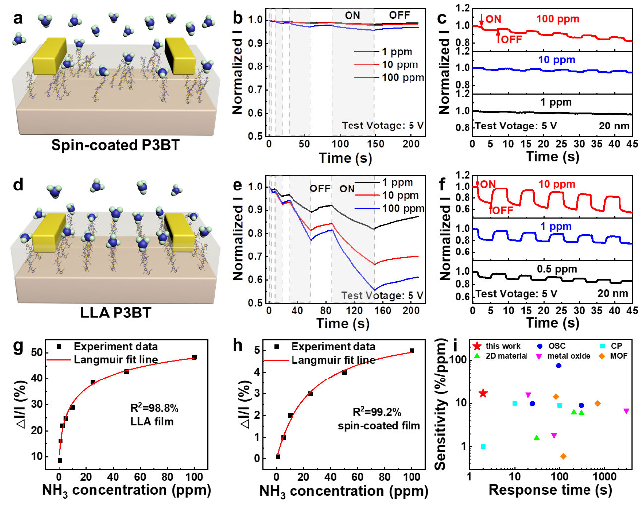
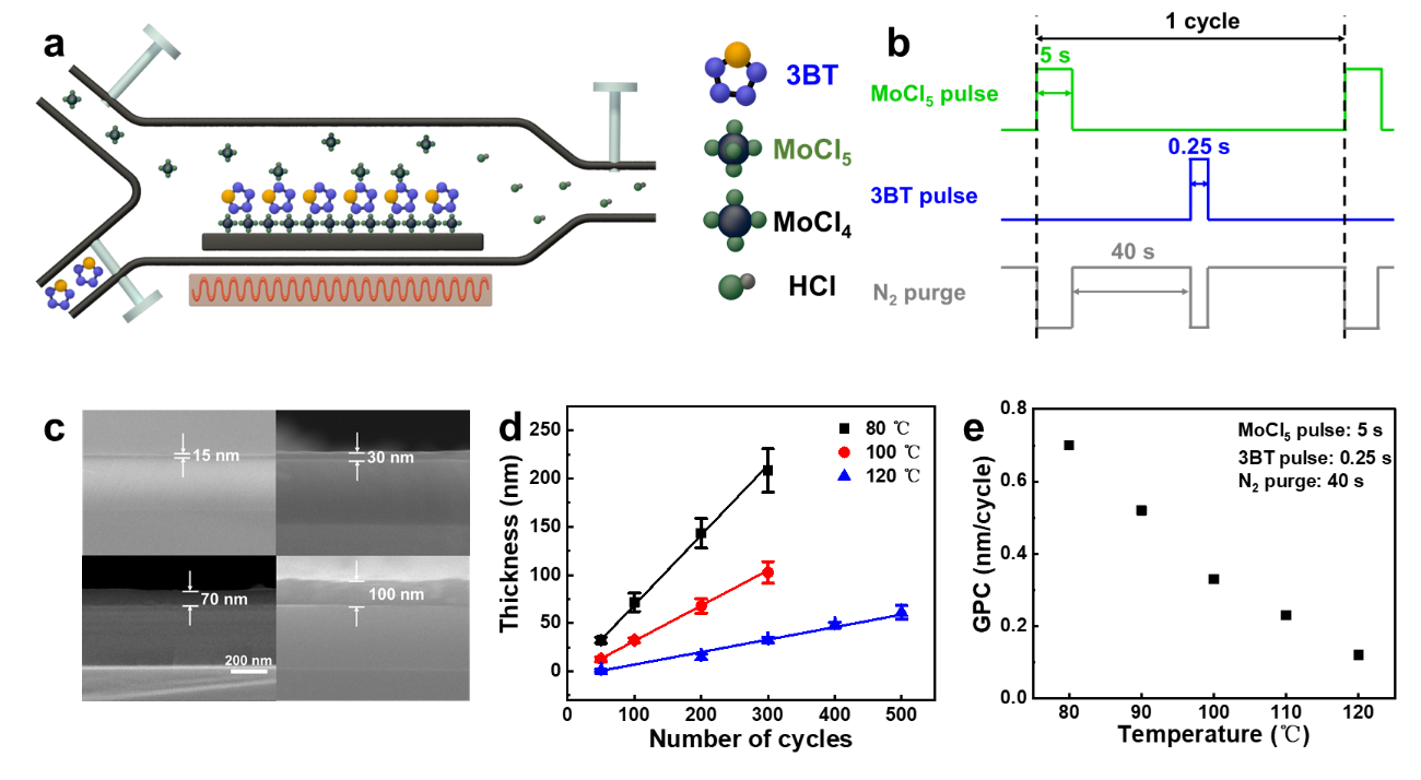
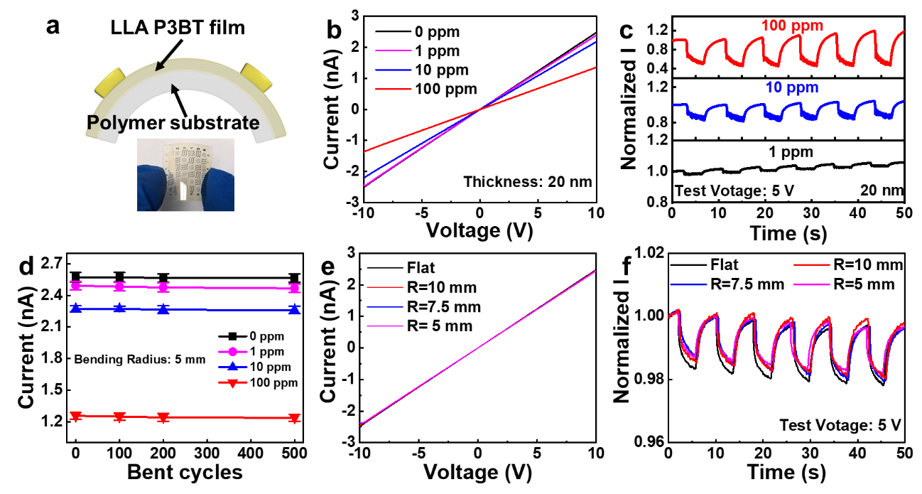
This layer-by-layer assembly process based on molecular layer deposition method makes use of the oxidative polymerization mechanism of thiophene groups, through the combination of chemical adsorption and physical adsorption, the thickness of polythiophene film increases linearly relative to the number of process cycles (Figure 1). Compared with the polythiophene films prepared by traditional spin coating process, the ultrathin films prepared by molecular layer deposition have obvious advantages in thickness uniformity and film continuity. In this paper, based on the in-depth analysis of the composition of the film, the process mechanism of the process is revealed in detail. The prepared ammonia sensor shows excellent response speed and sensitivity, which belongs to the best performance of similar devices reported (Figure 2). In addition, the molecular layer deposition of polythiophene thin films can also be applied to flexible polymer substrates, and the developed devices show good ammonia sensitivity and mechanical flexibility (Figure 3).
Original link: https://pubs.acs.org/doi/10.1021/acs.chemmater.1c02182
In September 2020, our group reported a color perception device based on spectral projection
Using the bandgap-gradient perovskite as the photoconductive channel, our research group developed a new device that can directly detect the spectral/color information of optical signals. The work was published online in the journal under the title “Spectrum projection with a bandgap-gradient perovskite cell for color perception”. The journal is a subordinate journal of Nature publishing group, and the latest impact factor is about 14. Corresponding authors are Shijin Ding, a researcher in the school of Microelectronics, Fudan University, and Xiaohan Wu, an associate researcher. The first author is Meina Zhang, a master student. Collaborators include professor Yongfeng Mei, Department of Materials Science, Fudan University; Dr. Antoine Riaud, young researcher, School of Microelectronics; and Dr. Fengxian Xie, young researcher, School of Information Science and Engineering.

Original link: https://www.nature.com/articles/s41377-020-00400-w
The 2019 ALD symposium in China and the ALD exchange meetin between China and South Korea was successfully held in Huangshan on August 10-12, 2019
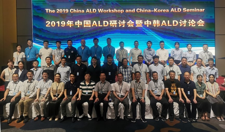
The 2019 ALD symposium in China and the ALD exchange meetin between China and South Korea was successfully held in Huangshan on August 10-12, 2019. This conference is mainly for professors and researchers engaged in ALD research in China and South Korea, dozens of invited teachers introduced their latest research results. Including the application of ALD in the preparation of two-dimensional materials and new nanomaterials, the development new ALD processes such as selective ALD growth process, organic molecule MLD growth process, and the development of new ALD equipment, etc. The atmosphere of the meeting was warm and the experts had an in-depth exchange and discussion, and announcing that the next international ALD technology application conference will be held in Wuhan Donghu hotel on October 11-14, 2020.
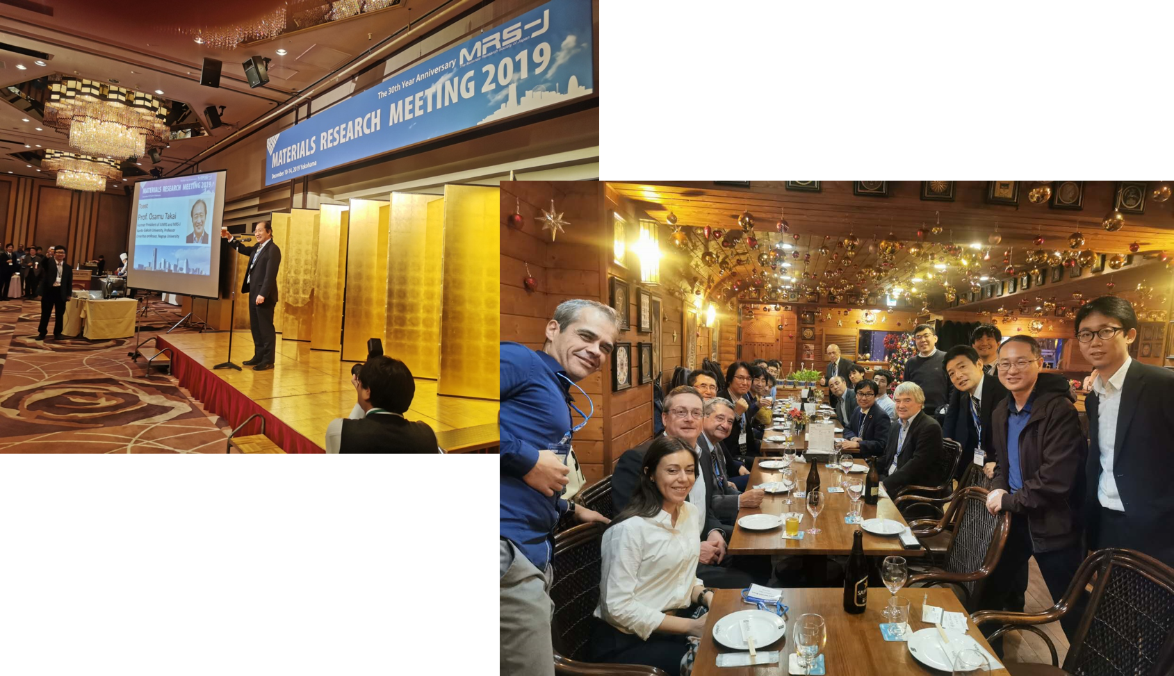
In 2019, professor Shi-Jin Ding was invited to attend the Materials Research Meeting in Yokohama, Japan
In 2019, professor Shijin Ding was invited to attend the Materials Research Meeting in Yokohama, Japan and make the Invited Talk, titled “Amorphous IGZO Thin-Film Transistors with AIOx:H Dielectrics for Emerging Functional Applications”. The recent achievements of the research group in light detection and synaptic devices are introduced. During the meeting, friendly exchanges were held with experts from Europe, America and Asia.
